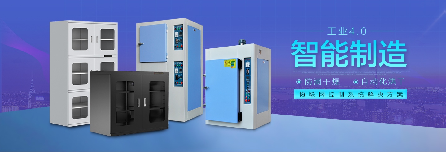
Drying or curing of organic substrates, adhesives, encapsulants, underfills, inks or coatings is one of the key processes in the manufacturing or assembly of advanced and mature semiconductor packages.
Improperly executed, the curing process often results in downstream yield and reliability issues, resulting in rework costs and order delays. Perhaps the lack of focus on curing is due to the relatively low capital and labor costs traditionally spent in the field. Due to the curing process Improper management and control may bring about many unfavorable quality problems.Part 2 introduces the process and technical advice. Based on several key points, in choosing ICpackageSemiconductor ovenshould be carefully considered.
Typical quality issues in the curing process include:
1.Material contamination
Outgassing of volatiles from organic materials in the product during heating can precipitate or deposit on clean surfaces of subassemblies in the curing chamber. By selecting low outgassing sealants or adhesives, and by increasing the rate of air exchange and emissions within the curing chamber frequency and\/ or volume, which can reduce or eliminate this problem.Therefore, the oven should have the function of program control, and perform actions such as exhaust and ventilation according to the process requirements.
2.Before the baking process is over, open the door to feed in and out
Interrupting the curing process to enter or exit small batches of product may contaminate product stored nearby or pose a health and safety risk to operators working nearby. Product nearby should be stored in a sealedElectronic moisture-proof cabinetMedium. The area around the curing equipment should be fully ventilated. Do not open the oven during the curing process, otherwise the batch of baked products may be scrapped.
3.Oxidation
Heating processes such as curing or drying may oxidize metallized areas, orPads for electrical interconnection on an IC die or substrate - coppersubstrateincreasingly used forThe preferred metallization for electrical interconnects in IC packaging. One of the disadvantages of copper is that it tends to form stubborn oxides that are difficult to remove or penetrate, so care must be taken to prevent their formation. Atmosphere controls oxide thickness.Nitrogen-filled and oxygen-free is a common condition for semiconductor packaging ovens, and oxygen-free conditions can also be achieved by vacuum. The main difference between the two is cost.
4.material stress
Large differences in thermomechanical properties between adjacent materials in the package can lead to high stress gradients that can lead to delamination at the interface and lead to cracking of the package. These conditions can cause electrical interconnects to be lifted or severed, and cause significant damage to the electrical interconnects.The IC die itself causes mechanical damage. The stress level increases with the size of the IC die.therefore need2-step curing profile with tightly controlled heating and cooling rates.It is very necessary to adhere to a strict heating curve.
becauseICThe package has a specific process, select the appropriateICpackage,semiconductorovenis controlICA crucial step in the curing process. With program control, cooling, oxygen-free conditions, etc., can meet theIC\/Semiconductor packaging requirements.
