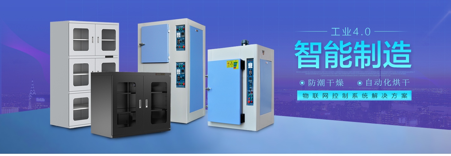
typicalThe IC package assembly process consists of many process steps, many of which require drying or curing, also need to useSemiconductor oven. These curing steps are usually125Celsiusto175Celsiusin the oven at various temperaturesbake1 to 6 hours.
1.Substrate Baking: The assembly process begins with a curing step that bakes the pin grid arrayPotential moisture in organic substrates for (PGA), ball grid array (BGA) and chip scale (CSP) packages.
2.Underfill curing:flip chipAfter the (FC) die is soldered to the substrate, the gap between the IC die surface and the substrate is "underfilled" with a low viscosity, 2 silicon oxide filled epoxy to reduce thermal expansion coefficient mismatch between dies and layers Press the base plate.
3.Heat sink curing:Increased power dissipation and reduced die size are driving the attachment of heat sinks to packages andGrowing demand for the backside of FC dies. Many different adhesive materials, available in liquid (or paste) and film (or preform) form, are used for this application.
4.Mold Bonding and Curing:In most wire bondsIn (WB) applications, an IC die is bonded to a metal leadframe or laminate substrate. The adhesive contains filler particles that make it conductive or insulating, depending on whether electrical biasing or thermal properties are required on the backside of the die Connection. In multi-die and stacked die applications, die bonding and curing operations may be repeated 2 to 5 times.
5.Coating curing:Coating can be used to protectIC chips are protected from corrosion by ionic impurities in molding compounds,The process of coating long, fine pitch wire bonds to prevent wire sweeps and electrical shorts on the die; the process of spin coating resist.
6.Package curing:haveCOB applications for WB or FC interconnects are typically encapsulated with a liquid, 2-silicon oxide filled epoxy material dispensed from a syringe. The blocked area is filled with a lower viscosity self-leveling epoxy to cover and protect the chip. For filling Material-wise, it is critical to achieve good, void-free adhesion to the dam material and underlying components. The fill material must remain level with the top of the dam material throughout the curing process.
7.Glue curing:Liquid sealants are also used to encapsulate optical components such asLED lights and displays, as well as many large electronic component enclosures.
8.post-mold curing:Most packages contain a singleIC chip and WB interconnect, followed by transfer molding using a thermoset epoxy molding compound. The pelletized compound is injected into the hot mold to form the body around the IC mold and cured in the mold for 1 to 2 minutes. Release from the mold back,packagerequires an additional curing process, known as post-mold curing,
9.mark dry:Most marking inks in use today either use UV light(UV) light curing, or heat curing. They are formulated with good adhesion and solvent resistance.
10.Dry Pack Bake: In Ship Moisture SensitiveBefore IC packaging, they are thoroughly dried or baked and sealed in airtight bags in an operation called dry packaging. IfIC absorb moisture from the atmosphere, they are likely to experience package cracking during subsequent circuit board assembly processingCase.
For different process stages, considering process requirements, capacity requirements and economy, different ovens can be selected to apply. Including possibleOxygen-free oven(substrate baking, solid crystal baking),vacuum oven(vacuum defoaming baking, wafer baking), ordinary blast precision oven (dehumidification and drying of finished products), double-door flat-bottom oven (batch curing and baking).