Semiconductor manufacturing can be subdivided into two process steps, front and back. The first process is to process silicon materials into wafers, and load the IC design patterns on the wafers through multiple processes such as photolithography machine exposure to make integrated circuits; the latter process is to process the wafers with integrated circuits Divide into basic units, and make final integrated circuit products after packaging and testing.
Semiconductor chip production workshops have very strict production conditions control, constant temperature, constant humidity and strict air dust particle size control and electrostatic protection measures. Only exposed chips will not be installed under such strict environmental control. Invalidate.
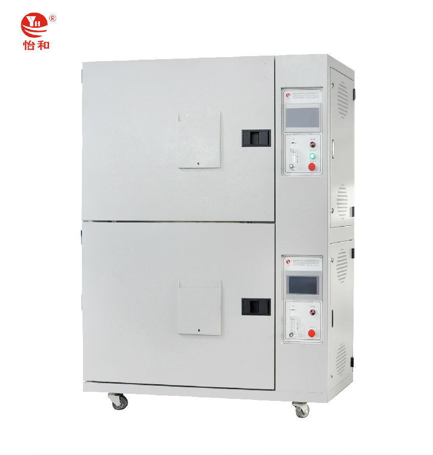
The semiconductor packaging oven is used in large quantities, the structure is becoming more and more complicated, and the performance requirements are gradually improved. It is used in a large amount before and after the packaging process, and it has become one of the important equipment in the process of intelligence and automation.
The semiconductor wafer oven developed by Yee Hing can perform front-end semiconductor functions such as wafer-level burn-in and magnetic annealing, as well as assembly/wafer-level encapsulation functions (such as die bond curing, stability and burn-in tests, and thermal shock) ) To meet its annealing, drying and thermal decomposition requirements, as well as to meet the requirements of clean technology, low oxidation, and efficient curing of adhesives and polymers in large-scale semiconductor packaging and assembly production.

