As one of the high-end manufacturing fields in the future, the development of semiconductors is highly concerned by the market. Benefiting from the downstream demand drive of multiple application scenarios such as the Internet of Things and intelligent high-end, its stand-alone automation is no longer a problem, and the intelligence and informatization of the overall factory are the main demands of customers.
In the semiconductor production process, photolithography is an important process link in the pattern transfer of integrated circuits. The quality of the coating directly affects the quality of the photolithography, and the coating process is also particularly important. In the photoresist coating process, most photoresists are hydrophobic, and the hydroxyl groups and residual water molecules on the surface of the silicon wafer are hydrophilic, which results in poor adhesion between the photoresist and the silicon wafer, especially the positive glue. During development, the developer will invade the joints between the photoresist and the silicon wafer, which can easily cause bleaching, floating glue, etc., resulting in the failure of the photolithographic pattern transfer, and the wet etching is prone to lateral corrosion. Tackifier HMDS (hexamethyldisilazane) can improve this situation well. After HMDS is applied to the surface of the silicon wafer, it can be reacted to produce a compound with siloxane as the main body after heating. It successfully changed the surface of the silicon wafer from hydrophilic to hydrophobic, and its hydrophobic base can be combined with the photoresist well and act as a coupling agent.
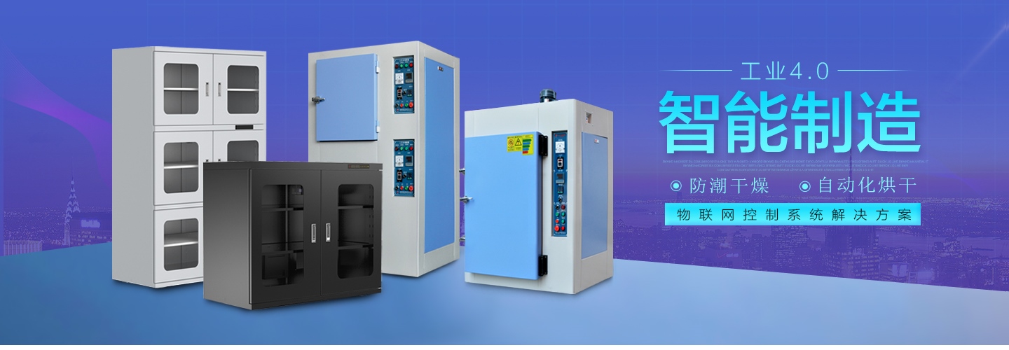
As an enterprise with automated production equipment and non-standard customized equipment, Yihexing is committed to providing customers with high-tech, cost-effective production equipment and supporting solutions around the mission of "meeting industrial needs". The self-developed photoresist high-temperature curing oven, semiconductor high-temperature oven is used in the special process requirements of precision electronic components, photoresist curing, and dust-free drying of electronic ceramic materials. The air in the box is closed and self-circulating, and it is filtered by high-temperature and high-efficiency air. The filter (level 100) is repeatedly filtered to keep the working chamber of the oven in a dust-free state. The dust-free oven studio is of stainless steel structure. It is suitable for touch screen, wafer, LED, PCB board, ITO glass and other precision electronics, solar energy, new materials and other industries.
