Chip-on-board packaging (COB) has become more widely used. The semiconductor chip is transferred and mounted on the PCB board, and the electrical connection between the chip and the substrate is realized by a wire stitching method, and a resin cover is used to ensure stability. The main welding methods of COB are hot pressure welding, ultrasonic welding and gold wire welding. COB packaging process expansion, adhesive, placement, heat binding, dispensing, curing, post-test.
In the packaging process of electronic products, the critical value of oxidation is different due to the different properties of each product. However, when the storage environment humidity is ≤5%RH, for most electronic materials, the corrosion reaction no longer exists. Because the humidity environment below 5% RH is equivalent to a vacuum state, it is isolated from the influence of moisture on all grades of chips and wafers, and will not be affected by moisture no matter how long the storage is.
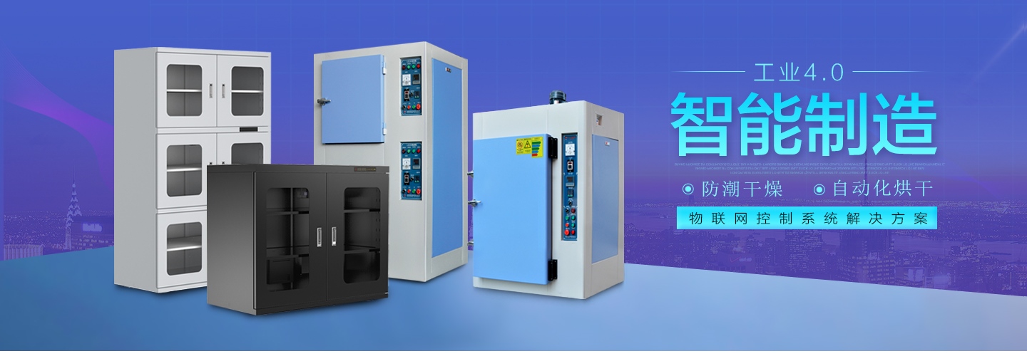
According to GB/T 14264-2009 semiconductor material terminology, GB/T 25915.1-2010 clean room and environmental requirements, since wafers are extremely easy to oxidize, the storage environment requires an oxygen-free environment. The main function of the nitrogen tank is to ensure that the materials are not oxidized during the storage process and to ensure the success rate of the materials.
In fact, nitrogen has been used for oxidation prevention in the production process of the electronics industry for a long time. A considerable number of companies have confirmed the scientificity and safety of the ultra-low humidity storage method. LED chip packaging and product applications have now formed a relatively complete industrial chain. In this industrial chain, moisture-proof and anti-oxidation applications are indispensable. Therefore, nitrogen cabinets are a must-have choice for the electronics industry.
